close
Choose Your Site
Global
Social Media
Modern home appliance PCBs serve as the vital brains powering today's connected electronics and automation systems. This article explores how advanced PCB layout design integrates IoT connectivity modules (such as Wi-Fi and Bluetooth) and smart sensors directly into household devices. It examines the manufacturing balance between high-density SMT assembly and rugged through-hole techniques, ensuring maximum circuit reliability against heat and moisture. By transitioning toward multilayer PCBs and flexible substrates, engineers can successfully optimize production costs, boost energy efficiency, and deliver the compact, durable architectures required for next-generation smart homes.
Optimizing a power supply PCB is vital for achieving high efficiency, power integrity, and strict electrical safety in modern electronics. This article explores essential PCB design practices, comparing the low-noise stability of linear supplies with the compact efficiency of switched-mode power supplies (SMPS). It highlights critical strategies for thermal management—such as utilizing thermal vias and wide copper pours—and layout techniques for EMI suppression, decoupling, and low-impedance grounding. By adhering to industry benchmarks like IPC-2221, engineers can eliminate hotspots, prevent electrical hazards, and build robust power regulation systems.
Printed Circuit Boards (PCBs) are foundational to the efficiency, thermal management, and lifespan of modern LED lighting systems. This article outlines how specialized substrates—such as Metal Core PCBs (MCPCBs) with aluminum or copper bases and ceramic PCBs—excel at heat dissipation compared to standard FR-4 materials. By incorporating key design strategies like thermal vias, optimized copper thickness, and integrated driver circuitry, engineers can successfully eliminate hotspots, reduce EMI, and prevent premature LED failure. Ultimately, choosing the correct PCB material and assembly method ensures optimal brightness, durability, and energy efficiency across diverse automotive, consumer, and industrial applications.
Effective PCB thermal management is vital for maximizing electronic reliability and system efficiency. This article explores how PCB material selection directly influences heat dissipation, comparing the thermal conductivity, Tg, and CTE of standard FR4, high-Tg laminates, and Metal Core PCBs. It highlights critical layout design strategies, including optimizing component placement, utilizing copper pours, and incorporating thermal vias to eliminate damaging hotspots. Ultimately, balancing material costs with specific thermal requirements enables engineers to prevent overheating and ensure long-term device longevity.
Selecting the right PCB material—whether FR4 PCB, CEM-1 PCB, or Aluminum PCB—is essential for optimizing an electronic design's performance, durability, and cost. FR4 serves as the rigid, flame-retardant industry standard capable of supporting complex multilayer designs. CEM-1 offers a highly cost-effective, lightweight alternative restricted to simple single-layer circuits due to its paper-composite core. Meanwhile, Aluminum PCBs excel in high-power applications like LED lighting by providing unmatched thermal management and mechanical robustness through a heat-dissipating metal core. Engineers must balance these distinct thermal, mechanical, and budget trade-offs early in the design phase.
CEM-1 PCBs offer a highly cost-effective substrate solution for budget-sensitive, single-layer electronic designs. Composed of a paper-based core reinforced with a single woven glass fabric layer and epoxy resin, this material delivers reliable electrical insulation and moderate mechanical durability for low-frequency consumer electronics, LED lighting, and educational prototyping. However, its lower thermal resistance and single-layer limitation make it unsuitable for high-frequency or complex multilayer circuits. Ultimately, CEM-1 serves as an affordable, eco-friendly choice with reduced energy consumption during manufacturing, balancing performance and sustainability for simple circuit applications.
Choosing the right PCB material is critical for project reliability. This article provides a comprehensive comparison between Aluminum PCBs and FR4 PCBs, highlighting their structural differences, costs, and applications. Aluminum PCBs feature a metal core that provides exceptional thermal conductivity and mechanical strength, making them ideal for high-power applications like LED lighting. Conversely, FR4 PCBs utilize a fiberglass epoxy substrate that excels in electrical insulation, cost-effectiveness, and complex multilayer designs for consumer electronics. Ultimately, the selection depends on balancing your project's specific thermal constraints, routing complexity, and budget requirements.
Choosing the right PCB Material is essential for ensuring the performance, reliability, and lifespan of electronic products. This guide compares common PCB materials, including FR-4, CEM-1, CEM-3, Polyimide, Aluminum, Copper, Ceramic, and Rogers, highlighting their properties, advantages, applications, and limitations. It also explains the key factors to consider when selecting PCB materials, such as thermal management, mechanical strength, signal integrity, and operating frequency, helping engineers choose the most suitable material for different electronic applications.
Use a criteria checklist to vet PCB manufacturers: audit technical limits, quality control, scalability. Avoid delays & hidden costs.
Standard FR4 PCB: When it works, when it fails. Learn to balance cost, thermal limits, and avoid prototype failures with proper material selection.
Specify and source Aluminum PCBs confidently: guide covers thermal management, dielectric specs, DFM, and vendor selection for high-power applications.
Struggling to choose between CEM-1 and FR4 PCB? Learn when to specify each substrate to balance cost, reliability, and layer count for your design.
Select PCB substrates to prevent thermal failure and signal loss. Balance electrical, thermal, mechanical properties. Plus supply chain realities.
Green: Most common, low cost; good UV light transmission, beneficial for exposure process; high contrast of lines, easy to detect defects.Black:earance is high-end, but low reflectivity, difficult for visual inspection; slightly higher heat absorption (extremely small impact on heat dissipation)Whit
PCBs power nearly every modern device, making the PCB circuit board the backbone of today's electronics. In 2025, demand is shifting toward smaller, faster, greener, and smarter designs that redefine performance and sustainability.
In today's world, every device hides a secret hero. The PCB circuit board connects and powers all components. From smartphones to medical devices, modern life depends on them. In this article, you'll discover why PCBs are essential to innovation and reliability in electronics.
Do you know why a PCB circuit board glossary matters? Misunderstanding key terms can cause design mistakes and costly delays. Knowing the right words speeds up work between engineers, buyers, and manufacturers. In this article, you will learn clear definitions and explanations of essential PCB terms.
In today’s fast-paced technological world, having a reliable and high-performance PCB (Printed Circuit Board) is crucial to ensure the functionality and longevity of electronic devices. Our custom PCB solutions are tailored to meet the needs of industries ranging from high-end power supplies to audi
OSP (Organic Solderability Preservative)Advantages:Low cost: Simple process, material cost is only 1/5 of gold plating.High flatness: Surface roughness <0.3μm, suitable for high-density SMT mounting.Environmental friendliness Does not contain heavy metals, complies with RoHS standards.Disadvantages:
As the world moves towards sustainability, our company is committed to reducing environmental impact without compromising on quality. Our PCBs are manufactured using eco-friendly materials and processes, ensuring that we contribute to a greener future while providing high-quality, durable products f
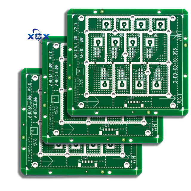
The Multilayer Circuit Board (Multilayer PCB) is an advanced printed circuit board design featuring multiple copper conductive layers laminated together with insulation.
It enables high circuit density, signal integrity, and compact layouts—perfect for modern telecommunication, automotive, medical, aerospace, and industrial control systems.
At XRX PCB, we provide custom multilayer PCB manufacturing services with full engineering support, from 4-layer prototypes to 20-layer HDI boards.
Our in-house production ensures tight tolerance, high reliability, and competitive lead times for your complex electronic designs.
| Feature | Description | Benefit |
|---|---|---|
| Layer Options | 4 to 20 layers | Supports complex circuit routing & signal control |
| High-Density Interconnect (HDI) | Microvia & blind/buried via technology | Enables compact, lightweight designs |
| Controlled Impedance | Maintains signal stability | Ideal for high-speed data transmission |
| Thermal Management | Multi-prepreg lamination & balanced copper | Ensures heat dissipation in power circuits |
| Precision Alignment | Automated optical layer registration | Guarantees inner layer consistency |
| Full Quality Inspection | AOI, flying probe test, impedance check | 100% reliability verification |
Multilayer PCBs play a critical role across a wide range of industries:
| Industry | Application | Benefit |
|---|---|---|
| Telecommunication | Routers, 5G base stations, signal processors | High-speed, low-loss transmission |
| Automotive Electronics | ECU, ADAS, EV battery management | Lightweight & heat-tolerant design |
| Medical Devices | Imaging systems, monitoring equipment | Stable signal integrity & miniaturization |
| Aerospace & Defense | Navigation, radar, satellite systems | Extreme reliability & vibration resistance |
| Industrial Automation | PLCs, motor controllers, sensors | Long operational life under harsh conditions |
| Consumer Electronics | Smart devices, IoT products | Compact structure, low EMI interference |
Our multi-layer PCBs are widely used across various industries:
Telecommunications: Routers, switches, signal processors
Industrial Control Systems: PLCs, automation equipment
Medical Devices: Imaging equipment, monitors, diagnostic tools
Aerospace: Avionics and control systems
High-End Consumer Electronics: Smartphones, tablets, wearable devices
These boards provide superior signal integrity, improved EMI shielding, and efficient space utilization, enabling designers to implement high-density circuits reliably.
| Parameter | Specification / Range | Description |
|---|---|---|
| Base Materials | FR-4, High-Tg FR-4, CEM-3, Rogers, Aluminum Core | Suited for different thermal & frequency needs |
| Layer Count | 4–20 Layers | Multilayer lamination for high-density boards |
| Board Thickness | 0.6 mm – 3.2 mm | Customizable based on layer stack-up |
| Copper Thickness | 1 oz – 3 oz | Higher copper weight supports power circuits |
| Min. Line Width / Spacing | 3 mil / 3 mil (0.075 mm) | Enables fine-pitch high-speed designs |
| Vias & Interconnections | Through-hole, Blind/Buried, Microvia | Advanced interlayer connectivity |
| Surface Finishes | ENIG, Immersion Gold, OSP, Lead-Free HASL | Enhances solderability & corrosion resistance |
| Solder Mask Colors | Green, Black, White, Blue, Red, Yellow | Custom for branding or function |
| Thermal Conductivity | 0.8 – 2.0 W/m·K | Ensures efficient heat transfer |
| Flame Retardant | UL 94V-0 Certified | Meets international fire safety standards |
| Testing | AOI, Flying Probe, Impedance, Cross-section Analysis | Full electrical & mechanical inspection |
| Certifications | ISO 9001, UL, RoHS, IPC-A-600 | Global quality and compliance standards |
| Typical Applications | Telecommunication, Automotive, Aerospace, Medical, Industrial Control, Power Systems | Suitable for compact, high-performance electronics |
Multilayer PCBs are designed for performance-critical electronic assemblies that demand both density and reliability.
They combine multiple signal layers with internal planes for power and grounding, reducing electromagnetic interference (EMI) and improving design stability.
Higher circuit density and smaller footprint
Improved signal integrity and EMI shielding
Excellent thermal balance and mechanical strength
Supports high-speed, high-frequency applications
Enhanced reliability with multiple dielectric layers
A perfect choice for advanced electronics, IoT devices, and compact embedded systems.
Advanced Manufacturing Capabilities: Precision etching, controlled lamination, and via formation
Material Flexibility: FR-4, high-Tg FR-4, Rogers, and high-frequency materials
OEM / ODM Support: Custom designs tailored to specific requirements
Quality Assurance: 100% testing for functionality and reliability, ISO and RoHS compliant
Fast Turnaround: From rapid prototyping to bulk production
A: A multi-layer PCB consists of three or more conductive layers separated by insulating materials, allowing for high-density and high-performance circuit designs.
A: As electronics become smaller and more complex, single and double-sided PCBs cannot meet space and performance requirements. Multi-layer PCBs allow for higher assembly density, reduced footprint, and improved EMI control.
A: We provide custom multi-layer PCBs up to 20 layers with precision impedance control.
A: FR-4, High-Tg FR-4, Rogers, and other high-frequency materials are available depending on your application.
A: Yes, we offer rapid prototyping and mass production, ensuring flexibility for development and production phases.
Looking for high-density, reliable multi-layer PCBs for your advanced electronics project?
Contact XRXPCB today to get a custom solution, fast lead times, and competitive pricing.
The Multilayer Circuit Board (Multilayer PCB) is an advanced printed circuit board design featuring multiple copper conductive layers laminated together with insulation.
It enables high circuit density, signal integrity, and compact layouts—perfect for modern telecommunication, automotive, medical, aerospace, and industrial control systems.
At XRX PCB, we provide custom multilayer PCB manufacturing services with full engineering support, from 4-layer prototypes to 20-layer HDI boards.
Our in-house production ensures tight tolerance, high reliability, and competitive lead times for your complex electronic designs.
| Feature | Description | Benefit |
|---|---|---|
| Layer Options | 4 to 20 layers | Supports complex circuit routing & signal control |
| High-Density Interconnect (HDI) | Microvia & blind/buried via technology | Enables compact, lightweight designs |
| Controlled Impedance | Maintains signal stability | Ideal for high-speed data transmission |
| Thermal Management | Multi-prepreg lamination & balanced copper | Ensures heat dissipation in power circuits |
| Precision Alignment | Automated optical layer registration | Guarantees inner layer consistency |
| Full Quality Inspection | AOI, flying probe test, impedance check | 100% reliability verification |
Multilayer PCBs play a critical role across a wide range of industries:
| Industry | Application | Benefit |
|---|---|---|
| Telecommunication | Routers, 5G base stations, signal processors | High-speed, low-loss transmission |
| Automotive Electronics | ECU, ADAS, EV battery management | Lightweight & heat-tolerant design |
| Medical Devices | Imaging systems, monitoring equipment | Stable signal integrity & miniaturization |
| Aerospace & Defense | Navigation, radar, satellite systems | Extreme reliability & vibration resistance |
| Industrial Automation | PLCs, motor controllers, sensors | Long operational life under harsh conditions |
| Consumer Electronics | Smart devices, IoT products | Compact structure, low EMI interference |
Our multi-layer PCBs are widely used across various industries:
Telecommunications: Routers, switches, signal processors
Industrial Control Systems: PLCs, automation equipment
Medical Devices: Imaging equipment, monitors, diagnostic tools
Aerospace: Avionics and control systems
High-End Consumer Electronics: Smartphones, tablets, wearable devices
These boards provide superior signal integrity, improved EMI shielding, and efficient space utilization, enabling designers to implement high-density circuits reliably.
| Parameter | Specification / Range | Description |
|---|---|---|
| Base Materials | FR-4, High-Tg FR-4, CEM-3, Rogers, Aluminum Core | Suited for different thermal & frequency needs |
| Layer Count | 4–20 Layers | Multilayer lamination for high-density boards |
| Board Thickness | 0.6 mm – 3.2 mm | Customizable based on layer stack-up |
| Copper Thickness | 1 oz – 3 oz | Higher copper weight supports power circuits |
| Min. Line Width / Spacing | 3 mil / 3 mil (0.075 mm) | Enables fine-pitch high-speed designs |
| Vias & Interconnections | Through-hole, Blind/Buried, Microvia | Advanced interlayer connectivity |
| Surface Finishes | ENIG, Immersion Gold, OSP, Lead-Free HASL | Enhances solderability & corrosion resistance |
| Solder Mask Colors | Green, Black, White, Blue, Red, Yellow | Custom for branding or function |
| Thermal Conductivity | 0.8 – 2.0 W/m·K | Ensures efficient heat transfer |
| Flame Retardant | UL 94V-0 Certified | Meets international fire safety standards |
| Testing | AOI, Flying Probe, Impedance, Cross-section Analysis | Full electrical & mechanical inspection |
| Certifications | ISO 9001, UL, RoHS, IPC-A-600 | Global quality and compliance standards |
| Typical Applications | Telecommunication, Automotive, Aerospace, Medical, Industrial Control, Power Systems | Suitable for compact, high-performance electronics |
Multilayer PCBs are designed for performance-critical electronic assemblies that demand both density and reliability.
They combine multiple signal layers with internal planes for power and grounding, reducing electromagnetic interference (EMI) and improving design stability.
Higher circuit density and smaller footprint
Improved signal integrity and EMI shielding
Excellent thermal balance and mechanical strength
Supports high-speed, high-frequency applications
Enhanced reliability with multiple dielectric layers
A perfect choice for advanced electronics, IoT devices, and compact embedded systems.
Advanced Manufacturing Capabilities: Precision etching, controlled lamination, and via formation
Material Flexibility: FR-4, high-Tg FR-4, Rogers, and high-frequency materials
OEM / ODM Support: Custom designs tailored to specific requirements
Quality Assurance: 100% testing for functionality and reliability, ISO and RoHS compliant
Fast Turnaround: From rapid prototyping to bulk production
A: A multi-layer PCB consists of three or more conductive layers separated by insulating materials, allowing for high-density and high-performance circuit designs.
A: As electronics become smaller and more complex, single and double-sided PCBs cannot meet space and performance requirements. Multi-layer PCBs allow for higher assembly density, reduced footprint, and improved EMI control.
A: We provide custom multi-layer PCBs up to 20 layers with precision impedance control.
A: FR-4, High-Tg FR-4, Rogers, and other high-frequency materials are available depending on your application.
A: Yes, we offer rapid prototyping and mass production, ensuring flexibility for development and production phases.
Looking for high-density, reliable multi-layer PCBs for your advanced electronics project?
Contact XRXPCB today to get a custom solution, fast lead times, and competitive pricing.