
close
Choose Your Site
Global
Social Media
Views: 0 Author: Site Editor Publish Time: 2026-06-17 Origin: Site
Specifying the right materials bridges the gap between theoretical electrical design and physical manufacturing reality. You cannot treat substrate selection as an afterthought. Incorrect choices often lead to severe consequences. These include signal degradation, thermal failure, excessive fabrication costs, or critical supply chain delays. A design might look flawless in a software simulation but fail instantly on the test bench. We see this happen frequently when engineers overlook environmental or fabrication constraints. This guide provides a pragmatic, engineering-focused framework. You will learn how to evaluate and select substrates properly. We base this approach on actual application requirements, manufacturing limitations, and real-world availability. You will discover how thermal, electrical, and mechanical properties dictate absolute performance limits. Finally, we will help you align your layout choices with practical supply chain realities to ensure successful, repeatable production runs.
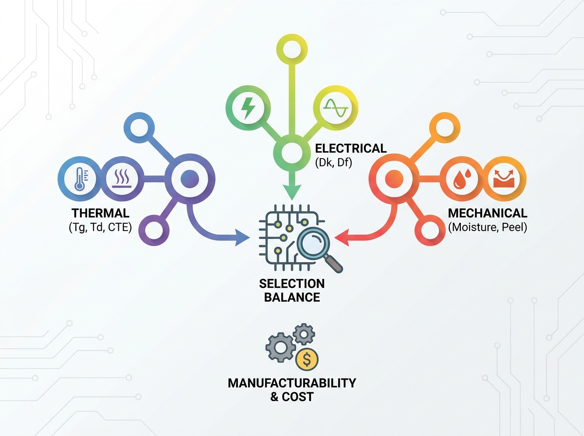
Base material selection on a balanced evaluation of thermal survivability (Tg, Td), electrical performance (Dk, Df), and mechanical stability (CTE).
Avoid over-specifying; standard FR-4 is highly capable for most baseline applications, while advanced high-frequency laminates should be reserved for strict signal integrity requirements.
Specify materials by their IPC-4101 standard (slash sheets) rather than exclusive brand names to mitigate supply chain bottlenecks and reduce lead times.
Fabricator capabilities must align with material choices—advanced substrates often require specialized drilling, lamination, and handling processes that impact final yield and cost.
You must evaluate substrates across three primary categories. These include thermal properties, electrical properties, and mechanical stability. Failing to balance these factors often causes catastrophic board failures during assembly or field deployment. Let us break down the critical metrics you need to analyze.
Heat acts as the primary stressor for printed circuit boards. Boards face extreme thermal shocks during the soldering process. They also endure long-term thermal cycling in their operating environments. You must carefully specify limits for thermal survivability.
Glass Transition Temperature (Tg): This represents the point where a rigid substrate shifts into a pliable, rubbery state. It does not indicate melting. Instead, it marks a critical change in structural integrity. You must establish the baseline Tg needed for your operating environment. Standard FR-4 offers a Tg around 130°C. Lead-free soldering processes usually require a Tg greater than 150°C. High-reliability designs often push this requirement above 170°C.
Decomposition Temperature (Td) & Coefficient of Thermal Expansion (CTE): Td measures the exact temperature where the material permanently degrades. It loses 5% of its total mass at this point. CTE evaluates how much the material expands under heat. We pay close attention to Z-axis expansion. Excessive Z-axis expansion during reflow tears the copper inside plated through-holes (PTH) and vias. You must select materials exhibiting low CTE to guarantee via reliability.
Electrical metrics dictate how signals travel across your board. These properties become aggressively important as operating frequencies increase.
Dielectric Constant (Dk): Dk determines how the material affects signal propagation speed. A lower Dk allows signals to travel faster. You must emphasize Dk stability across your entire operational frequency range. Materials often exhibit shifting Dk values as frequencies rise. This shift ruins controlled impedance calculations and destroys signal integrity.
Dissipation Factor (Df) / Loss Tangent: Df measures how much signal energy the dielectric absorbs. The substrate turns this absorbed energy into heat. Minimizing insertion loss remains non-negotiable for high-speed digital and RF designs. Standard FR-4 has a relatively high Df. Advanced laminates offer ultra-low Df values to preserve weak RF signals.
Environmental factors severely impact bare board performance. You cannot ignore mechanical strength or chemical resistance in your analysis.
Moisture Absorption Rates: Substrates absorb water from humid environments over time. Water carries a massive dielectric constant of roughly 80. Even a tiny amount of absorbed moisture destroys your carefully calculated Dk profile. High moisture absorption also increases the risk of delamination during wave soldering. The trapped water rapidly turns into steam and blasts the board layers apart.
Peel Strength: This metric assesses the bond strength between the copper foil and the dielectric base. High peel strength is particularly important for heavy copper power boards. Mechanical stresses and thermal cycling weaken this bond over time. A weak bond causes copper pads to lift right off the board surface during component rework.
| Property Category | Key Metric | Primary Impact on Design |
|---|---|---|
| Thermal | Tg (Glass Transition) | Determines survivability during lead-free assembly. |
| Thermal | CTE (Expansion Rate) | Dictates mechanical reliability of vias and through-holes. |
| Electrical | Dk (Dielectric Constant) | Controls signal speed and trace impedance geometry. |
| Electrical | Df (Dissipation Factor) | Impacts signal loss over distance at high frequencies. |
| Mechanical | Moisture Absorption | Affects long-term electrical stability and delamination risk. |
Engineers often face the temptation to over-specify substrates. Choosing the highest-rated laminate guarantees performance but destroys project budgets. You should match the material directly to the application demands.
Standard FR-4 variants dominate the industry for good reason. They offer an excellent balance of cost, manufacturability, and baseline electrical performance. FR-4 works perfectly for most digital logic, microcontrollers, and low-frequency analog circuits.
In highly cost-sensitive scenarios, composite materials like CEM-1 and CEM-3 prove entirely sufficient. These composites replace woven glass fabric with a cellulose paper core. You often see them deployed in low-complexity, high-volume production. A great example includes a standard Single-Sided PCB used in consumer appliances. Basic LED lighting modules and cheap power adapters also rely heavily on CEM materials to maintain strict profit margins.
Gigabit-speed communication infrastructure requires entirely different material classes. Standard FR-4 simply absorbs too much signal energy above a few gigahertz.
You must evaluate PTFE-based and ceramic-filled laminates for these applications. Well-known examples include materials from Rogers and Taconic. These advanced substrates focus on strict Dk tolerances and ultra-low Df requirements. They provide consistent performance across extreme bandwidths. Antennas, automotive radar systems, and high-frequency RF transceivers absolutely require these premium dielectrics to function correctly.
Power converters and motor controllers generate massive amounts of concentrated heat. The substrate must aggressively pull heat away from active components.
Engineers analyze Metal Core PCBs (MCPCB) and heavy-copper FR-4 for thermal management. MCPCBs utilize an aluminum or copper backing plate covered by a thin, thermally conductive dielectric. Automotive LED headlamps heavily rely on this technology. Rapid heat dissipation remains the primary success criterion here. Heavy copper boards utilize very thick copper planes (often exceeding 3 ounces) to carry massive currents while spreading thermal loads evenly.
Aerospace, military, and medical devices operate under unforgiving conditions. A failure in these sectors often risks human life.
These applications frequently utilize Polyimide and specialized high-Tg materials. Polyimide resists extreme temperature cycling and harsh chemical exposure. It also serves as the primary base for flexible circuits. High-reliability sectors demand materials proven to survive decades of continuous vibration, vacuum exposure, or repeated sterilization cycles.
Signal integrity becomes incredibly fragile in the gigahertz realm. Every physical aspect of the board acts as an unwanted component. You must carefully manage the interaction between signals and substrate physics.
Lower Dk and Df materials cost significantly more than standard options. You need a clear framework for determining when a transition becomes technically justified. Upgrading your PCB Materials purely for safety margins wastes money.
Generally, designs operating below 1 GHz function perfectly on standard FR-4. When frequencies cross the 2 to 3 GHz threshold, dielectric losses become highly problematic. Trace length also dictates this decision. A 10 GHz signal might survive a very short trace on FR-4. However, routing that same signal across ten inches requires an advanced low-loss laminate. You must simulate insertion loss to justify the higher material costs.
High-frequency signals do not travel evenly through a copper trace. They get pushed to the outer edges of the conductor. We call this phenomenon the skin effect. Because the signal rides strictly along the copper surface, the physical profile of the foil matters immensely.
Standard copper foil features a rough microscopic profile to improve adhesion to the dielectric. This roughness acts like a bumpy road for high-frequency signals. It forces the current to travel a longer path, increasing resistance and signal loss. You must specify Reverse Treated (RT) or Ultra-Low Profile (ULP) copper foils for microwave designs. Smoother copper dramatically reduces skin effect losses but requires specialized pressing techniques to prevent delamination.
Advanced laminates often cost three to five times more than standard FR-4. Building a 12-layer board entirely out of PTFE ruins project economics. We propose using a hybrid stack-up strategy instead.
A hybrid stack-up uses high-performance dielectrics only on the signal-critical layers. You route your high-speed RF lines on the outer layers using a premium Rogers core. You then utilize standard FR-4 for the remaining internal core layers handling power, ground, and low-speed digital routing. This strategy drastically lowers costs while preserving signal integrity exactly where it counts.
Selecting a brilliant material means nothing if your factory cannot buy it. Procurement bottlenecks ruin product launch schedules constantly. You must design for supply chain resiliency from day one.
Engineers often define a stack-up using a very specific brand and part number. Current market realities make this extremely dangerous. Relying entirely on one specific material brand halts production immediately if their stock runs out. Natural disasters, chemical shortages, or shipping embargoes routinely disrupt niche laminate supplies. You should never allow your design to depend on a single manufacturer's proprietary blend unless absolutely necessary.
We recommend a standard practice to avoid single-sourcing traps. You should call out IPC-4101 slash sheets on your fabrication drawings instead of brand names. The IPC-4101 standard categorizes base materials by their physical and electrical properties.
For example, noting "IPC-4101/126" specifies a high-Tg, RoHS-compliant FR-4 material. It does not demand a specific brand. This allows your manufacturer to source an equivalent material from their currently available inventory. They can swap brands seamlessly while guaranteeing the thermal and electrical performance you requested. This simple documentation trick mitigates massive supply chain bottlenecks.
Procurement timelines stretch drastically when you request unusual material configurations. You must understand how your specifications impact delivery dates.
Non-standard Thicknesses: Requesting a highly unusual core thickness forces the vendor to special-order the laminate. Stick to common metric or imperial thicknesses whenever possible.
Heavy Copper Weights: Standard foil weights like 1oz or 2oz remain abundant. Requesting 4oz or 6oz copper significantly limits your pool of immediate suppliers.
Specialty Dielectrics: PTFE and ceramic-filled cores rarely sit in massive quantities on local warehouse shelves. Selecting these niche materials automatically extends your procurement timelines by several weeks.
Fabricator capabilities must align perfectly with your material choices. Advanced substrates require specialized handling. They behave very differently on the factory floor compared to basic FR-4.
Mechanical drilling accounts for a large portion of fabrication time. High-performance materials significantly complicate this process. Ceramic-filled laminates act essentially like sandpaper. They wear down tungsten-carbide drill bits incredibly fast. High-Tg materials also resist drilling, requiring slower feed rates to prevent smearing. This increased wear forces the manufacturer to replace drill bits more frequently. It increases total fabrication time and drives up tooling costs substantially. You must account for these hidden manufacturing expenses.
Pressing different materials together requires deep expertise. Hybrid stack-ups present unique thermal challenges during the lamination cycle.
Differing Melting Points: PTFE and FR-4 require vastly different temperatures to flow and bond properly. The factory must design a custom thermal profile to cure both simultaneously.
CTE Mismatches: Dissimilar materials expand at different rates inside the press. This CTE mismatch introduces massive internal stresses. It severely increases the risk of board warpage as the panel cools down.
Registration Issues: Different materials shrink differently after pressing. Maintaining perfect alignment for micro-vias across a hybrid boundary challenges even advanced fabricators.
You cannot send an advanced PTFE design to a factory optimized for basic consumer boards. Emphasize the necessity of verifying vendor capabilities early. You must ensure your chosen manufacturer has the specific pressing equipment required. They need specialized plasma-etching chemistry lines to desmear advanced laminates properly. Always verify their prior experience with your selected material before submitting your final Gerber files.
The ideal substrate selection balances electrical necessity with budget realities and supply chain health. Over-specifying materials wastes immense capital, while under-specifying guarantees catastrophic field failures. You must evaluate thermal thresholds, electrical signal demands, and mechanical stability holistically.
To ensure project success, follow these specific next steps. First, define your highest operating frequency and longest trace route to evaluate insertion loss risks. Next, confirm your operating environment temperatures to set a strict baseline for Tg and Td. Finally, engage with your manufacturing partner during the early layout phase. Validating stack-up assumptions and material stock before finalizing your design prevents costly delays and ensures a smooth transition into volume production.
A: The general threshold sits around 2 to 3 GHz. Standard FR-4 exhibits higher dielectric loss, which attenuates high-frequency signals. However, this depends heavily on your specific FR-4 grade and total trace lengths. Very short traces might survive higher frequencies, while long routes require advanced laminates earlier.
A: Rarely. Changing a material generally introduces a different dielectric constant (Dk). This alteration shifts your trace impedance parameters. You will likely need to recalculate and adjust your trace widths and spacing geometry to maintain correct controlled impedance.
A: Tg (Glass Transition Temperature) marks the softening point where a rigid material becomes pliable and rubbery. Td (Decomposition Temperature) marks the permanent degradation point where the material breaks down chemically and loses 5% of its total mass.
A: Water possesses an extremely high dielectric constant (roughly 80). When a substrate absorbs ambient moisture, the water severely degrades the material's intended electrical performance. It heavily alters impedance profiles and drastically increases signal loss in high-frequency applications.


