close
Choose Your Site
Global
Social Media
Views: 0 Author: Site Editor Publish Time: 2025-09-18 Origin: Site
Ever wondered how the tiny circuits inside your gadgets are made? PCB circuit board PCB circuit board are the backbone of modern electronics, enabling devices to function seamlessly. In this post, you'll learn how PCB design and manufacturing have evolved to meet 2025's technological demands.
In 2025, the drive for smaller, more powerful devices pushes PCB designs toward miniaturization. High-Density Interconnects (HDI) play a crucial role by allowing more connections in a compact space. This means fitting more components on a smaller board without sacrificing performance.
Manufacturers use advanced surface mount technology (SMT) and microvias—tiny holes that connect layers—to achieve this. For example, smartphones and medical devices benefit from HDI because they need to be lightweight yet packed with features. HDI boards can have up to 20 or more layers, increasing routing capacity significantly.
Automation is no longer optional; it's essential. AI-powered systems now handle many manufacturing steps, including automated optical inspection (AOI) and robotic soldering. These technologies speed up production and reduce errors.
AI also analyzes production data to optimize workflows, minimizing waste and improving quality control. For instance, AI algorithms can detect defects earlier than human inspectors, ensuring higher yield rates. This trend enables manufacturers to meet high-volume orders while maintaining strict quality standards.
The rise of wearable tech and IoT devices fuels demand for flexible and rigid-flex PCBs. These boards use bendable substrates like polyimide, allowing them to conform to curved or moving surfaces.
Applications include smartwatches, medical monitors, and automotive sensors. Flexible PCBs reduce device size and improve user comfort. Manufacturers focus on durability and performance, ensuring these boards withstand repeated bending and harsh environments
Tip: To stay competitive, PCB manufacturers should invest in AI-driven automation and HDI technologies, enabling efficient production of smaller, more complex, and flexible circuit boards.
In 2025, PCB circuit boards increasingly rely on advanced substrates to meet higher performance demands. Traditional FR4 fiberglass remains popular for many applications due to its balance of cost and reliability. However, high-frequency and high-speed designs often require specialized materials like PTFE (Teflon) or ceramic substrates that offer low dielectric constants and minimal signal loss.
These high-performance substrates support faster signal transmission and better thermal stability. For example, Rogers 4350B is widely used in RF and 5G PCBs because it maintains consistent electrical properties up to 10 GHz frequencies.
Conductive inks have also evolved, enabling additive manufacturing techniques. These inks, often silver or copper-based, allow precise circuit patterns to be printed directly onto flexible or rigid substrates. This method reduces waste and supports rapid prototyping. Conductive inks also enable innovative applications like printed antennas and sensors integrated into wearable electronics.
3D printing technology is transforming PCB manufacturing by allowing complex, multi-dimensional circuit structures. Unlike traditional flat PCBs, 3D printed boards can have circuits on curved or irregular surfaces. This capability opens new possibilities for compact devices and embedded systems.
Specialized 3D printers deposit conductive inks and insulating materials layer by layer with micron-level precision. This process reduces material waste and accelerates prototyping cycles. For instance, aerospace and medical industries benefit from 3D printed PCBs tailored to unique form factors.
Though still emerging, 3D PCB printing offers cost-effective small-batch production and customization. As printer resolution and materials improve, expect broader adoption across consumer electronics and IoT devices.
Sustainability drives PCB innovation in 2025. Manufacturers prioritize biodegradable and eco-friendly materials to reduce environmental impact. Bio-based substrates derived from natural fibers or resins replace traditional petrochemical-based laminates in some applications.
Lead-free solders, halogen-free flame retardants, and recyclable copper layers are increasingly standard. These materials comply with stricter global regulations like RoHS and REACH, helping companies avoid penalties and appeal to environmentally conscious customers.
Some PCBs now incorporate compostable substrates that degrade safely after use, ideal for disposable electronics or short-lifespan IoT sensors. Eco-friendly manufacturing processes also reduce energy consumption and chemical waste.
Tip: To enhance PCB sustainability and performance, manufacturers should explore high-performance substrates combined with conductive inks and invest in 3D printing technologies that minimize waste and support complex designs.
The manufacturing journey starts with design and verification. Engineers use specialized software to create detailed PCB layouts. These layouts act like blueprints, showing where every trace, via, and component will go. The design must meet electrical, mechanical, and manufacturing rules to ensure it works properly and can be built efficiently.
Verification involves checking the design for errors, such as short circuits or spacing issues, using automated tools. This step also includes Design for Manufacturing (DFM) reviews, which confirm the design fits the capabilities of the chosen fabrication process. Early collaboration with manufacturers helps avoid costly mistakes and redesigns.
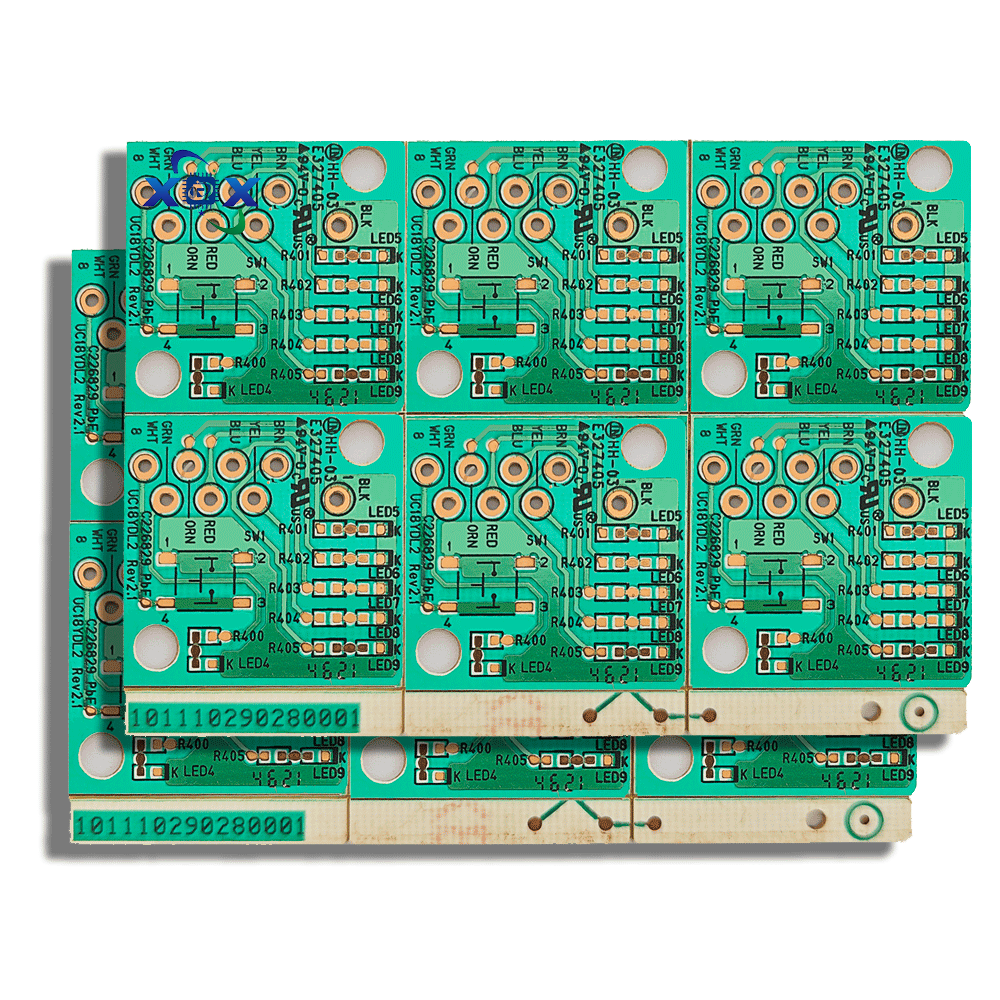
After design approval, the manufacturing moves to layer preparation. Multilayer PCBs consist of several thin layers of copper and insulating material stacked together. Precise alignment of these layers is essential. Registration holes guide this process, ensuring each layer lines up perfectly.
Once stacked, automated optical inspection (AOI) checks the layers for defects like misalignments, missing traces, or unwanted copper. AOI uses cameras and software to compare the physical layers against the design files. Detecting errors early prevents defective boards from continuing through production.
Next, the board undergoes plating and copper deposition. Drilled holes, called vias, connect different layers electrically but start as empty spaces. The plating process coats the hole walls with copper, creating conductive paths between layers.
The entire board surface also receives additional copper plating to build up trace thickness. This step improves electrical performance and durability. Various plating methods, such as electroless copper deposition, ensure uniform coverage even in tiny vias.
After plating, the board is cleaned and prepared for outer layer imaging and etching, which define the final circuit patterns.
Tip: Engage manufacturers early during design to align specifications with fabrication capabilities, reducing errors and speeding up production cycles.
Printed Circuit Boards (PCBs) serve as the backbone of countless electronic devices, making them vital in various industries. In 2025, their applications continue to expand, driven by evolving technology and increasing demand for smarter, more connected products. Here, we explore key sectors where PCBs play a crucial role.
Consumer electronics remain the largest market for PCBs. Devices like smartphones, laptops, tablets, gaming consoles, and smart home appliances rely heavily on advanced PCB designs. Miniaturization and high-density interconnects allow manufacturers to pack more features into compact devices without sacrificing performance. For example, modern smartphones often contain multilayer HDI PCBs that support 5G connectivity, high-resolution cameras, and powerful processors.
Wearable technology, such as fitness trackers and smartwatches, also depends on flexible PCBs that conform to curved surfaces. These boards must be durable and lightweight to ensure comfort and long-term use. As consumers demand more functionality and connectivity, PCB manufacturers innovate to meet strict size, power, and thermal requirements.
The automotive industry increasingly integrates electronics for safety, navigation, and entertainment. Electric vehicles (EVs) and autonomous driving systems require sophisticated PCBs capable of handling high voltages, extreme temperatures, and electromagnetic interference. Rigid and rigid-flex PCBs provide the mechanical stability and reliability needed in these harsh environments.
Aerospace systems demand PCBs that meet rigorous standards for durability, weight, and thermal resistance. Aircraft avionics, communication systems, and control units rely on multilayer PCBs made from specialized substrates to withstand vibration, radiation, and temperature extremes. For instance, satellites and spacecraft use PCBs designed for long-term operation in space, featuring radiation-hardened materials.
Medical devices increasingly incorporate PCBs to enable precise diagnostics, monitoring, and treatment. Devices like pacemakers, insulin pumps, and imaging equipment use PCBs that comply with strict safety and reliability standards. High-density and embedded component PCBs reduce device size while improving functionality.
The Internet of Things (IoT) drives demand for PCBs that support wireless communication, low power consumption, and sensor integration. Smart medical devices, wearable health monitors, and home automation systems rely on PCBs designed for seamless connectivity and data processing. Manufacturers focus on ensuring these boards provide stable performance over prolonged use and varying environmental conditions.
Tip: When designing PCBs for critical applications like automotive or medical devices, prioritize reliability and compliance with industry standards to ensure safety and performance.
Signal integrity is vital in PCB manufacturing, especially as devices grow smaller and faster. Poor signal quality can cause data errors or device malfunction. Designers tackle this by carefully controlling trace impedance, minimizing crosstalk, and reducing electromagnetic interference (EMI). Techniques include using controlled impedance traces, proper grounding, and shielding.
Thermal management is another critical challenge. Components generate heat that can degrade performance or shorten lifespan. Manufacturers use thermal vias, copper pours, and heat sinks to dissipate heat effectively. Materials with high thermal conductivity, like metal-core substrates, also help maintain safe operating temperatures.
For example, in high-speed digital circuits, maintaining signal integrity requires precise impedance control within ±5%. At the same time, thermal vias placed near heat-generating components reduce junction temperatures by up to 20°C, improving reliability.
Environmental regulations such as RoHS (Restriction of Hazardous Substances) and REACH (Registration, Evaluation, Authorization, and Restriction of Chemicals) impose strict limits on hazardous materials in PCBs. Manufacturers must use lead-free solders, halogen-free flame retardants, and eco-friendly substrates to comply.
Non-compliance risks fines, product recalls, and damage to brand reputation. To meet these standards, many companies adopt green manufacturing processes, including waste reduction, recycling copper scrap, and minimizing chemical use.
For instance, switching to lead-free solder alloys like SAC305 (tin-silver-copper) ensures compliance while maintaining solder joint reliability. Also, biodegradable substrates made from bio-based materials offer sustainable alternatives for disposable electronics.
Global supply chain disruptions affect PCB manufacturing by causing delays, material shortages, and cost increases. To mitigate risks, manufacturers diversify suppliers, maintain safety stock, and invest in local sourcing.
Advanced planning tools powered by AI help predict shortages and optimize inventory. Additionally, flexible manufacturing systems enable quick adaptation to changing material availability or design requirements.
An example is a manufacturer shifting from a single copper foil supplier to multiple regional sources, reducing lead times by 30%. Another strategy includes using 3D PCB printing for rapid prototyping when traditional materials face delays.
Tip: Prioritize early collaboration between design and manufacturing teams to address signal integrity, thermal challenges, and regulatory compliance, ensuring efficient production and product reliability.
AI is reshaping PCB design by automating complex tasks. It helps engineers optimize component placement, routing, and thermal management faster than ever. AI-driven tools analyze vast data sets, predicting potential design flaws early. This reduces costly iterations and accelerates time to market.
Quantum computing, though still emerging, promises to revolutionize PCB design. It can simulate electromagnetic fields and signal behavior at a scale classical computers struggle with. This capability enables designers to create circuits with unprecedented precision and efficiency. For example, quantum algorithms may optimize multilayer routing or minimize crosstalk in high-frequency boards.
Together, AI and quantum computing will push PCB innovation beyond current limits, enabling smarter, faster, and more reliable designs.
Industry 4.0 integrates digital technologies into manufacturing, making PCB production smarter and more flexible. Connected sensors and IoT devices monitor equipment in real-time, predicting maintenance needs and avoiding downtime. Automated guided vehicles (AGVs) and robotics streamline material handling and assembly.
Smart factories use AI-powered analytics to optimize production schedules, reduce waste, and improve quality control. For instance, automated optical inspection (AOI) systems detect defects with near-perfect accuracy, ensuring only flawless boards proceed.
This digital transformation enhances scalability and responsiveness, helping manufacturers meet growing demand while maintaining high standards.
The PCB market is set for robust growth, driven by sectors like 5G, electric vehicles, IoT, and medical devices. Experts predict the global market could exceed $100 billion by 2030, fueled by demand for advanced HDI, flexible, and embedded component boards.
Miniaturization and high-speed applications will require more complex multilayer designs, increasing manufacturing sophistication. Sustainability will also be a priority, with eco-friendly materials and energy-efficient processes becoming standard.
Manufacturers embracing AI, quantum computing, and Industry 4.0 will lead the market, offering innovative solutions at competitive costs.
Tip: Invest early in AI-driven design tools and Industry 4.0 technologies to future-proof PCB manufacturing and capitalize on emerging market opportunities.
In 2025, PCB circuit board design embraces trends like miniaturization, AI-driven automation, and eco-friendly materials. Staying updated with these innovations is crucial for manufacturers to remain competitive. The future of PCB boards involves AI, quantum computing, and Industry 4.0, promising smarter and more efficient designs. Companies like Xinrongxing lead the way by offering advanced PCB solutions, enhancing product performance and sustainability, and providing significant value to their customers.
A: A PCB circuit board, or Printed Circuit Board, is a vital component in electronic devices, providing a platform for electrical connections and components.
A: In 2025, PCB circuit boards are manufactured using AI-driven automation, HDI technologies, and advanced materials, improving efficiency and reducing errors.
A: Miniaturization allows PCB circuit boards to fit more components in smaller spaces, essential for compact devices like smartphones and medical equipment.
A: Flexible PCB circuit boards conform to curved surfaces, ideal for wearables and IoT devices, enhancing comfort and reducing device size.
A: AI optimizes PCB circuit board manufacturing by automating inspections and analyzing data, improving quality control and reducing waste.


