close
Choose Your Site
Global
Social Media
Views: 0 Author: Site Editor Publish Time: 2025-09-18 Origin: Site
In the world of electronics, PCB circuit boards are the unsung heroes. They form the backbone of countless devices, enabling complex functions in compact forms. Understanding what a PCB circuit board is and its importance in modern electronics is crucial for anyone interested in technology. In this guide, you'll learn the basics of PCB circuit boards and their vital role in powering our digital world."
A printed circuit board (PCB) is a flat board made from insulating material, usually fiberglass or composite epoxy. It serves as the foundation that holds and connects electronic components. Thin layers of copper traces are etched onto the board, creating pathways for electrical signals to flow between components. These traces act like tiny roads guiding electricity through the circuit.
The structure of a PCB typically includes several layers:
Substrate: The base layer, usually rigid and non-conductive, providing mechanical support.
Copper Layer: Conductive paths etched onto the substrate.
Solder Mask: A protective coating that insulates copper traces and prevents accidental solder bridges.
Silkscreen: Printed labels and markings to identify components and connections.
PCBs can be single-sided, with copper traces on one side, or double-sided, with traces on both sides. More complex PCBs have multiple layers stacked together, separated by insulating materials. These multilayer PCBs allow for compact designs with many connections.

PCBs come in various types depending on their construction and application:
| Type | Description | Common Use Cases |
|---|---|---|
| Single-sided | Copper traces on one side only. Simple and cost-effective. | Calculators, simple electronics |
| Double-sided | Copper traces on both sides, connected via drilled holes (vias). | Automotive dashboards, LED lighting |
| Multilayer | Multiple layers of copper and insulation laminated together. | Computers, smartphones, medical devices |
| Rigid | Made from solid, inflexible materials like FR-4 fiberglass. | Motherboards, industrial equipment |
| Flexible (Flex) | Made from bendable materials like polyimide film, can flex without damage. | Wearables, foldable phones |
| Rigid-flex | Combination of rigid and flexible sections in one board. | Aerospace, military, medical instruments |
| Metal-core | Uses metal as a base for better heat dissipation. | High-power LED lighting, motor controllers |
Each type offers unique benefits. For example, flexible PCBs save space and weight in compact devices, while metal-core PCBs help manage heat in power electronics.
Material choice affects PCB performance, durability, and cost. Here are common materials:
FR-4: Most widely used substrate; a fiberglass and epoxy composite. Offers good insulation and mechanical strength.
Polyimide: Flexible material used for flex PCBs; withstands high temperatures.
CEM (Composite Epoxy Material): A lower-cost alternative to FR-4, used in simpler boards.
Aluminum: Used in metal-core PCBs for excellent heat dissipation.
Ceramic: Provides high thermal conductivity, used in specialized high-frequency or high-power applications.
The copper layer thickness varies, typically measured in ounces per square foot. Standard PCBs use one ounce (about 35 micrometers thick), but high-power boards may use thicker copper for better current handling
Note: Choosing the right PCB type and materials early in the design process ensures optimal performance, reliability, and cost-efficiency for your electronic device.
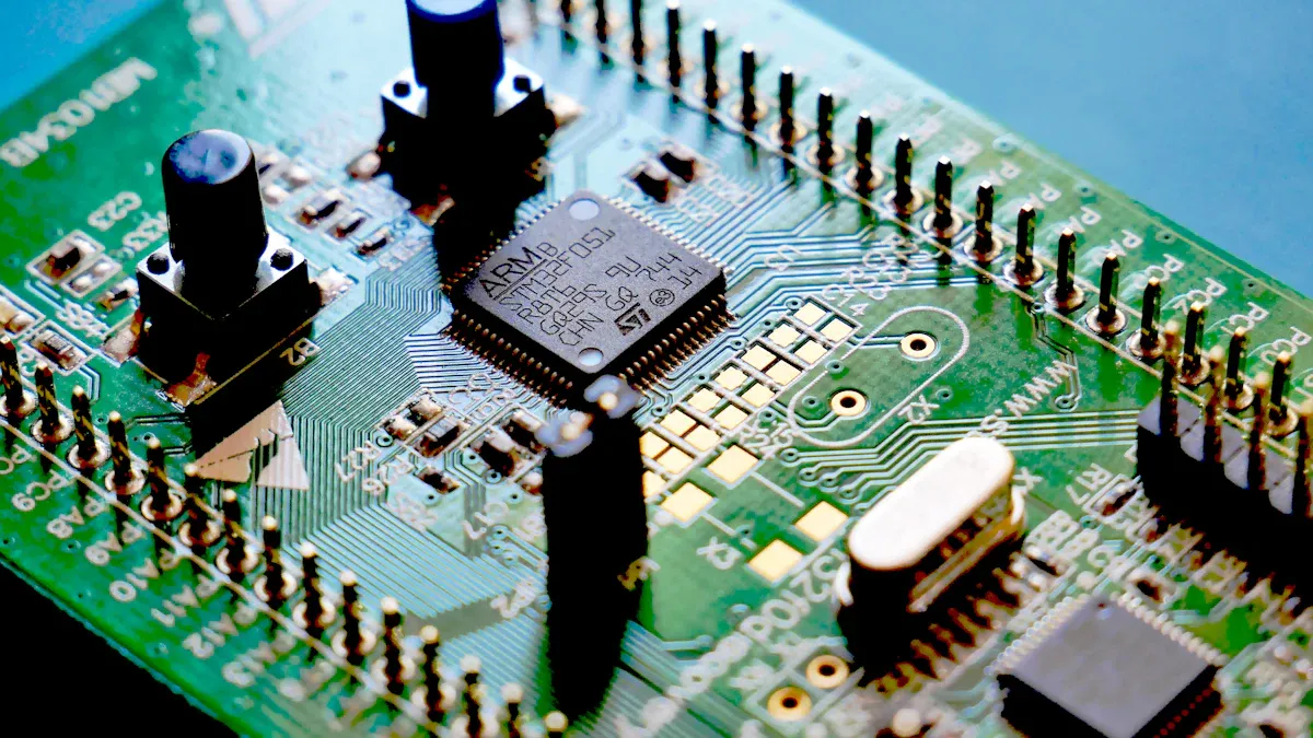
When you look at a printed circuit board (PCB), you’re seeing a finely crafted system made up of several key parts. Each part plays a special role to make sure the board works perfectly. Let’s break down these components.
PCBs hold two main types of electronic parts: active and passive.
Active components can control electric signals or generate energy. Examples include:
Transistors: Act as switches or amplifiers.
Diodes: Allow current to flow in one direction only.
Integrated Circuits (ICs): Tiny chips that perform complex tasks.
Sensors: Detect things like temperature or light.
Passive components don’t generate energy but store or regulate it. Examples are:
Resistors: Control the flow of electric current.
Capacitors: Store and release electrical energy.
Inductors: Store energy in a magnetic field.
Transformers: Transfer energy between circuits.
Together, these components form the heart and brain of the PCB, making it perform its intended function.
The PCB’s copper layers create the electrical pathways connecting components.
Traces are thin copper lines acting like roads for electric signals, guiding current between parts.
Pads are small copper areas where components get soldered onto the board.
Vias are tiny holes filled or plated with metal that connect traces on different layers of a multilayer PCB. They act like tunnels allowing signals to travel vertically through the board.
These features ensure all components communicate correctly and power flows where needed.
Two important layers protect and clarify the board’s surface:
Solder Mask: This is a thin, colored coating (usually green) covering the copper traces. It prevents accidental solder bridges during assembly and protects the copper from corrosion.
Silkscreen: Printed on top of the solder mask, this layer shows labels, symbols, and component outlines. It helps manufacturers and technicians identify and place parts accurately.
Tip: When designing or assembling a PCB, ensure solder mask openings precisely match pads to avoid soldering issues and maintain signal integrity.

Designing a printed circuit board (PCB) is a crucial step in creating any electronic device. It transforms a circuit idea into a physical layout that can be manufactured and assembled. This process involves careful planning and several stages: designing the schematic, simulating the circuit, placing components, and routing connections.
The PCB design process starts with a clear understanding of the circuit’s function. Engineers use specialized software called Electronic Computer-Aided Design (ECAD) tools. These tools help create precise layouts and ensure the board will work correctly once built.
The main stages include:
Creating the schematic diagram
Simulating the circuit’s behavior
Placing components on the board
Routing electrical connections (traces)
Reviewing design rules and preparing for manufacturing
Each step builds on the previous one, making sure the final PCB meets performance, size, and reliability requirements.
The schematic is a blueprint showing how all components connect electrically. Designers place symbols for parts like resistors, capacitors, and integrated circuits, then draw lines (nets) to represent connections.
Simulation tools test the schematic to catch errors early. They analyze how signals flow and verify that the circuit behaves as expected under different conditions. This step saves time and money by reducing costly mistakes during manufacturing.
Once the schematic is ready, it’s time to place components on the physical board. Placement affects signal integrity, heat dissipation, and manufacturability. Designers arrange parts to minimize trace lengths and avoid interference.
Routing connects the components using copper traces. These traces must follow design rules for width and spacing to handle current safely and prevent electrical noise. Designers also add vias—small plated holes—to connect traces across multiple board layers.
Good routing considers:
Signal path length and timing
Power and ground distribution
Minimizing electromagnetic interference (EMI)
Thermal management
Modern ECAD tools offer features like auto-routing and design rule checks to help designers achieve optimal layouts efficiently
Tip: Use simulation early in the design phase to validate your schematic and catch errors before moving to layout; this reduces costly redesigns and speeds up development.
Manufacturing a PCB starts with fabrication, where the board's physical form takes shape. The process begins by printing the PCB design onto a copper-clad substrate. This step uses a photoresist layer that protects parts of the copper during etching. Next, unwanted copper is chemically etched away, leaving only the copper traces that form the circuit pathways.
After etching, the board undergoes drilling to create holes for through-hole components and vias. These holes are precisely drilled to ensure good electrical connections between layers. Then, the board is layered and laminated if it's a multilayer PCB, bonding together the substrate, copper layers, and insulating materials under heat and pressure.
Following lamination, a solder mask is applied to protect the copper traces from oxidation and prevent solder bridges during assembly. Finally, silkscreen printing adds labels and markings to help identify components and connections on the board.
Once fabricated, the PCB moves to assembly, where components are attached. Two main techniques exist: through-hole and surface mount.
Through-Hole Assembly: Components have leads inserted into drilled holes on the PCB and soldered on the opposite side. This method provides strong mechanical bonds, making it ideal for components that endure mechanical stress or heat. It is common in connectors, large capacitors, and inductors.
Surface Mount Technology (SMT): Components are placed directly onto the PCB surface pads and soldered without drilling holes. SMT allows for smaller, lighter boards with higher component density, making it the preferred method for modern electronics. Automated pick-and-place machines position components quickly and accurately.
Often, manufacturers use a combination of both methods to optimize performance and cost.
Quality control ensures the PCB functions as designed and meets reliability standards. Testing starts with visual inspections to check for defects like solder bridges, misaligned components, or damaged traces.
Electrical testing follows, including:
In-Circuit Testing (ICT): Checks each component's presence and functionality by applying electrical probes to test points.
Flying Probe Testing: Uses movable probes to test connections without requiring custom fixtures, suitable for prototypes or small batches.
Functional Testing: Simulates the PCB’s operating environment to verify overall performance.
Advanced methods like X-ray inspection detect hidden solder joint issues, especially under ball grid array (BGA) components.
Quality control also involves verifying adherence to industry standards such as IPC-A-610, ensuring the PCB’s durability and safety
Tip: Choose the assembly technique early based on component size, mechanical strength needs, and production volume to optimize cost and reliability.
Printed circuit boards (PCBs) are everywhere in our modern world. They serve as the foundation for countless electronic devices across many industries. Let’s explore some of the most important applications of PCBs.
PCBs are the heart of most consumer electronics. Devices like smartphones, tablets, laptops, smartwatches, and gaming consoles all rely on PCBs to function. These boards connect tiny components such as microprocessors, memory chips, sensors, and power management circuits.
Consumer PCBs often use multilayer designs to fit complex circuits into small spaces. They also use surface-mount technology (SMT) to place components densely. The demand for thinner, lighter, and more powerful gadgets pushes PCB technology to evolve rapidly in this sector.
In automotive and aerospace industries, PCBs play critical roles in safety, control, and communication systems. Cars use PCBs in engine control units, infotainment systems, sensors, and advanced driver-assistance systems (ADAS). Electric vehicles especially depend on PCBs to manage battery systems and power electronics.
Aerospace applications require PCBs that withstand harsh environments like extreme temperatures, vibration, and shock. These boards are often rigid-flex or multilayer to meet strict reliability standards. They appear in navigation systems, avionics, satellite communications, and flight control units.
Medical devices need PCBs that are highly reliable and compact. Examples include pacemakers, MRI machines, diagnostic instruments, and wearable health monitors. These PCBs often use high-density interconnect (HDI) technology to pack many components into tiny spaces.
Industrial equipment relies on PCBs for automation, control, and monitoring. They appear in robotics, manufacturing machinery, power supplies, and sensors. Industrial PCBs are designed to endure high voltages, extreme temperatures, and mechanical stress
Tip: When designing PCBs for specific applications, consider industry standards and environmental conditions early to ensure durability and compliance.
Printed circuit boards (PCBs) continue evolving rapidly, driven by demand for smaller, faster, and smarter electronics. Let’s explore key trends shaping the future of PCB technology.
Devices keep shrinking, yet their capabilities grow. This drives the need for miniaturized PCBs with higher component density. High-Density Interconnect (HDI) technology enables placing more components in less space by using finer traces, smaller vias, and microvias. It supports complex circuits in smartphones, wearables, and medical implants.
Ultra-High-Density Interconnect (UHDI) PCBs push miniaturization further. They use advanced additive manufacturing to create extremely fine features. UHDI boards support cutting-edge processors and high-speed data transfer, ideal for AI devices and next-gen communications.
Material innovation plays a big role in PCB performance. Traditional FR-4 remains popular, but new materials improve thermal management, flexibility, and signal integrity.
Polyimide and Liquid Crystal Polymer (LCP): Used for flexible PCBs, offering excellent heat resistance and mechanical durability.
Ceramics: Provide superior thermal conductivity, ideal for high-frequency or power electronics.
Metal-Core Substrates: Aluminum or copper cores help dissipate heat in LED lighting and power modules.
High-Speed Laminates: Materials like Rogers and Teflon reduce signal loss and support high-frequency applications.
These materials allow designers to optimize boards for specific environments and performance needs.
The Internet of Things (IoT) revolution fuels PCB innovation. IoT devices require compact, low-power, and reliable PCBs to connect sensors, processors, and communication modules.
Smart devices often use multilayer HDI PCBs to pack functionality into tiny footprints. Flexible and rigid-flex PCBs enable wearable tech and foldable gadgets. Integration of wireless charging coils and antennas directly on PCBs is becoming common.
Additionally, IoT demands robust PCBs that can withstand varied environments, from industrial sensors exposed to heat and vibration to medical devices requiring biocompatibility
Tip: Embrace HDI and flexible PCB technologies early to stay competitive in markets driven by miniaturization and IoT innovations.
Assembling a PCB circuit board involves understanding its components and design, ensuring precise placement and routing for optimal performance. Staying updated with PCB technology is crucial for adapting to trends like miniaturization and IoT integration. Xinrongxing offers innovative PCB solutions, enhancing device functionality and reliability with advanced materials and techniques. Their products provide significant value by meeting industry standards and adapting to evolving technological demands, ensuring high-quality and efficient electronic devices.
A: A PCB circuit board is a flat board made from insulating material, usually fiberglass or composite epoxy, that holds and connects electronic components using copper traces.
A: Troubleshooting a PCB circuit board involves checking for visual defects, performing electrical tests like in-circuit testing, and using diagnostic tools to identify faulty components or connections.
A: PCB circuit boards provide a compact, reliable, and efficient way to organize and connect electronic components, ensuring stable performance and ease of manufacturing.
A: The cost of a PCB circuit board varies based on complexity, materials, and quantity, with prices ranging from a few cents for simple boards to several dollars for advanced designs.
A: Multilayer PCB circuit boards offer compact designs, increased connection density, and improved signal integrity, ideal for complex devices like computers and smartphones.


