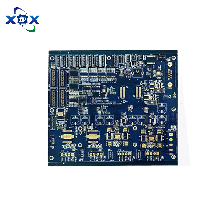
1、 Process technology
The core of double-sided PCB manufacturing lies in achieving double-sided wiring and interlayer conductivity, and its process flow is complex and requires precise control of key links:
1. Core process flow
Graphic electroplating method (mainstream process):
Copper clad laminate → Drilling → Chemical copper plating/electroplating (metalization of holes) → Pattern transfer (film coating/exposure) → Pattern electroplating (tin lead corrosion-resistant layer) → Etching → Film stripping → Solder mask printing → Surface treatment (such as gold deposition, tin spraying).
SMOBC process (bare copper overlay solder mask):
On the basis of graphic electroplating, an additional lead and tin removal step is added to solve the problem of solder bridging in thin lines, improving solderability and reliability.
Innovative processes (such as inkjet printing masks):
Adopting a trapezoidal conical hole design, anti etching ink is printed through inkjet printing to achieve both circuit patterning and via protection, reducing processes by 30% and lowering costs.
2. Key technical difficulties and
Solution to the causes of difficulties
Optimization of electroplating parameters for uneven chemical copper plating or rough hole walls due to through-hole metallization defects, using black hole/direct electroplating technology instead of chemical copper plating
Control the concentration of etching solution (such as ferric chloride+hydrochloric acid) by controlling the penetration of etching solution or electroplating diffusion for side etching and coating widening, and adjust the spray pressure
Insufficient thermal stability of the solder mask layer foaming substrate, and the use of non adhesive substrates (such as FR-4 fiberglass epoxy resin)
3. Environmental Trends
The traditional chemical copper plating process is gradually being replaced by environmentally friendly processes such as black hole technology and direct polymer electroplating due to cyanide pollution.
2、 Core advantages
1. Performance advantages
Improved wiring density: Double sided wiring supports complex circuit designs, saving 40% of area compared to single panels, and is suitable for high integration scenarios such as smartphone motherboards.
Excellent electrical performance: surface treatment with immersion gold technology reduces impedance, improves signal transmission efficiency by 30%, and has strong anti-interference ability.
Mechanical and thermal stability: The double-sided structure enhances seismic performance (in bumpy car environments) and evenly dissipates heat through a copper layer to avoid local overheating.
2. Cost and reliability
High cost-effectiveness: Mass production costs are 50% lower than multi-layer boards, with a low failure rate and easy maintenance.
Long life design: The surface treatment of immersion gold/spray tin is corrosion-resistant, and the service life can reach more than 10 years (industrial control equipment).
3. Limitations
Complexity limitation: The demand for ultra high speed or multi-layer interconnection needs to be upgraded to multi-layer boards.
High process threshold: The yield of through-hole metallization directly affects the overall reliability.
3、 Application Fields
Double sided PCBs dominate the following fields with high reliability and adaptability:
1. Communication and computing devices
5G router: Gold plating technology ensures low loss transmission of high-frequency signals.
Server control board: Double sided SiP packaging reduces module size by 40% and improves power efficiency.
2. Automotive Electronics
Electronic Control Unit (ECU): Anti vibration design ensures stable operation of the engine control board during bumps.
Car lights/wipers: OSP surface treatment is resistant to humid environments and has a lifespan of up to 8 years.
3. Medical equipment
CT scanner/monitor: High precision wiring supports weak signal acquisition, and the immersion layer prevents biological corrosion.
4. Consumer electronics
Smartphone/tablet: 6 × 6mm double-sided SiP module for high-density integration (such as PMIC power management).
LED driver board: simplifies wiring structure, reduces mass production costs by 25%.
5. Industry and Aerospace
Sensor/PLC controller: Wide temperature resistance range (-40 ℃~125 ℃), suitable for harsh factory environments.
Satellite communication module: Double sided gold-plated PCB maintains signal integrity at extreme temperatures.
Comparison Table of Application Fields:
The core advantages of typical products in the field reflect the process characteristics
Communication equipment 5G base station router high-frequency low loss, anti-interference gold surface treatment
Anti vibration and moisture resistant OSP/tin spraying process for automotive electronic ECU control board
Medical equipment CT scanner circuit high-precision signal acquisition laser drilling (aperture ≤ 0.1mm)
Consumer electronics, smartphones, motherboards, high-density integration, double-sided SMT mounting
Industrial control temperature sensor with wide temperature range stability and thick copper design (above 2oz)
4、 Industry Trends
Technological upgrade: Inkjet printing mask and trapezoidal via design promote process simplification and increase production efficiency by 20%.
Material innovation: The demand for flexible double-sided panels (thickness 0.1mm) in folding equipment and medical probes is increasing by 15% annually.
Market growth: The global double-sided PCB market will reach 39.6 billion US dollars by 2024, with China accounting for over 40% of the market