close
Choose Your Site
Global
Social Media
| Quantity: | |
|---|---|
XRX-102579
DGXRX
1. Detailed Explanation of Core Process Technology
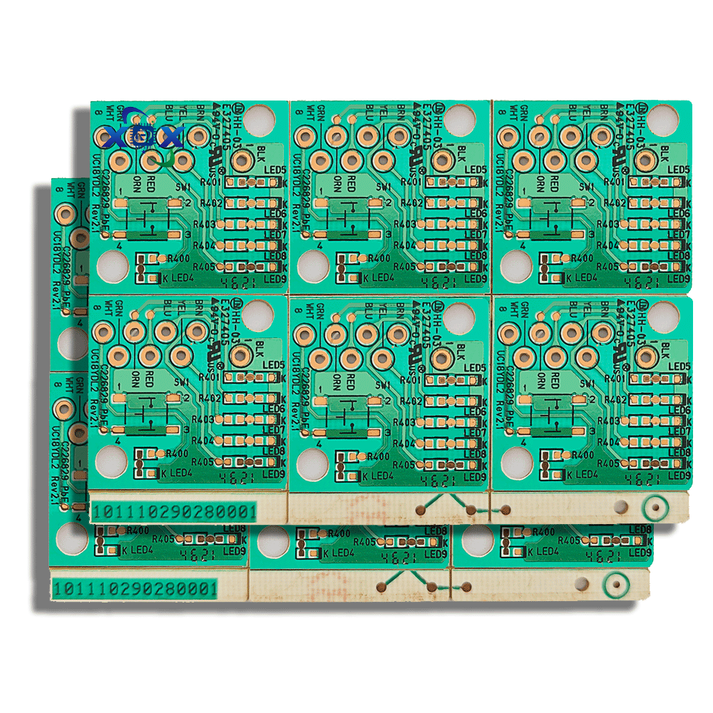
1. Standard Process (Through-Hole Metalization)
Process Key Technical Points Precision Requirements
Base Material Preparation FR-4/Aluminum substrate cutting, copper foil thickness 1-2oz (5-70μm) Size tolerance ±0.15mm
Drilling CNC mechanical drilling (hole diameter ≥0.3mm) → Dering Hole position accuracy ±0.05mm
Hole Metalization PTH (Chemical Plating): Palladium activation → Chemical electroplating0.5-1μm) → Electroplating thickening (hole copper ≥20μm) Deep diameter ratio ≤8:1
Graphic Double-sided LDI exposure → Graphic electroplating (copper tin protection) → Alkaline etching film removal Line width tolerance ±0.07
Solder Mask and Surface Treatment Screen printing/spraying solder mask ink (green oil) → Character printing → HASL spray tin/ENIG gold immersion/P anti-oxidation Solder mask bridge width ≥0.1mm
2. Advanced Process (High Reliability Scenarios)
Via resin filling
Fill through-holes with epoxy resin to prevent solder paste from infiltrating during welding (mandatory process for automotive electronics).
Selective gold plating:Local ENIG gold immersion (contact area) OSP treatment (soldering area), cost reduction of 40% compared to full-board gold immersion.
Thick copper design:
2oz copper foil etching on the outer layer, supporting large current (>10A) power modules.
2. Material Advantages Selection Guide
Comparison of Base Material Properties
Material Type Dielectric Constant (Dk) Thermal Conductivity (W/mK) Bending StrengthMPa) Applicable Scenarios
FR-4 Epoxy Board 4.3-4.7 0.3 >400 Consumer Electronics/ustrial Control Motherboard
CEM-1 Composite Board 4.5-5.0 0.25 >300 Low-cost Home Appl Control Board
Aluminum Substrate - 1.5-4.0 >200 LED Lighting/Automotive Power Module
Polytetrafluethylene 2.0-2.2 0.25 >150 High-frequency RF Module (<6GHz)
Golden Rules for Material:
Cost-effective First Choice: FR-4 (best comprehensive performance)
Heat Dissipation Necessity: Aluminum Substrate (60% in thermal resistance)
High-frequency Application: PTFE (Insertion loss <0.02dB@5GHz)
3. Core Advantage Analysis1. Electrical and Structural Performance
Indicator Double-sided Board Performance Comparison with Single-sided Panel Improvement
Wiring Density Supports cross-line, reducing jumpers Component density increased by 50%
Signal Integrity Controllable through-hole impedance (±8%), suitable for circuits below 50MHz Interference reduction of 20%
Heat Dissipation Capability Double-sided copper laying heat conduction via holes, thermal resistance reduction of 0% Temperature rise of 15℃ (equal power consumption)
Reliability Meets IPC-6012 CLASS 2 standard (ind grade) Lifespan >10 years (industrial environment)
2. Economic Advantages
Cost Efficiency Ratio:
40-60% lower than 4-layer boards, supporting moderately complex circuits (MCU systems/power management)
Batch production cycle of 3-4 days (30% faster thanayer boards)
Maintainability Convenience:
Fault points can be located through through-holes, repair success rate >90%
4. Application and Typical Cases
1. Consumer Electronics (50% share)
Smart Home:
WiFi module (ESP8266 double-sided board) Bluetooth speaker motherboard
Portable Devices:
Mobile power control board (2oz thick copper), e-book


