
close
Choose Your Site
Global
Social Media
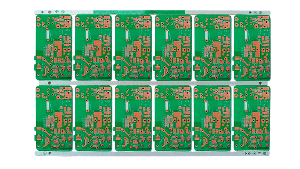

Our FR-4 double sided PCB features conductive circuitry on both sides of an FR-4 substrate, providing additional routing space for electronic designs that require more connections than a single-sided board can accommodate.
The listed configuration includes a 1.6 mm board thickness, 1 oz copper weight, green solder mask, and a minimum drilling hole size of 0.5 mm. Custom fabrication requirements can be reviewed according to your Gerber files, electrical requirements, and assembly specifications.
Product Highlights
Two-Sided Copper Circuitry
FR-4 Base Material
1.6 mm Board Thickness
1 oz Copper Weight
Green Solder Mask
| Quantity: | |
|---|---|
Parameter | Specification |
|---|---|
Product Name | FR-4 Double Sided PCB |
PCB Type | Double-Sided Rigid PCB |
Number of Conductive Layers | 2 |
Base Material | FR-4 |
Board Thickness | 1.6 mm |
Copper Weight | 1 oz |
Solder Mask Color | Green |
Minimum Drilling Hole Size | 0.5 mm |
The specifications above describe the currently listed product configuration. Other board dimensions, copper weights, drilling requirements, and surface finishes should be confirmed according to the design files and manufacturing requirements.
A double sided PCB uses conductive copper circuitry on both the top and bottom surfaces of an insulating substrate. This two-layer structure provides additional space for routing electrical connections and arranging electronic components.
Depending on the circuit design, plated through-holes or other specified interconnections can connect conductive features between the two sides. This allows designers to distribute circuit connections across both surfaces rather than routing every connection on a single layer.
For projects with more components, branching connections, or limited board space, a double sided PCB can offer greater layout flexibility than a single-sided design.
The final construction depends on the circuit layout, hole structure, electrical requirements, and approved fabrication data.
Conductive circuitry on both sides provides additional routing options for designs with multiple electrical connections.
Designers can distribute components and circuit traces across the top and bottom surfaces to accommodate different layout requirements.
FR-4 glass fiber reinforced epoxy laminate provides an insulating substrate for rigid PCB construction.
Compared with multilayer designs, a double sided PCB uses two conductive layers and can be suitable for projects that do not require additional internal circuit layers.
Board dimensions, copper weight, hole specifications, solder mask, and surface finish can be reviewed according to the intended application and design files.
Comparison Item | Single Sided PCB | Double Sided PCB |
|---|---|---|
Conductive Circuitry | One side | Both sides |
Routing Space | Limited to one conductive layer | Additional routing space |
Circuit Complexity | Suitable for simpler compatible layouts | Suitable for designs requiring more connections |
Component Layout | More constrained by one-sided routing | Greater layout flexibility |
Design Considerations | Layer count and routing simplicity | Interlayer connections and two-sided routing |
Typical Selection Factor | Simple circuit requirements | More complex routing or limited board space |
A single-sided PCB may be suitable when the complete circuit can be routed on one conductive layer. A double sided PCB provides more routing flexibility when the design requires additional connections.
The appropriate option depends on the circuit design, component density, electrical requirements, board dimensions, and manufacturing cost.
Double sided PCB manufacturing involves several interdependent specifications. The final configuration should be reviewed against the Gerber files before production.
Parameter | Available Reference / Option |
|---|---|
Base Material | FR-4; CEM-1 subject to board structure |
Board Thickness | Current product: 1.6 mm; other thicknesses subject to confirmation |
Copper Weight | Current product: 1 oz; 2 oz and 3 oz options listed in general factory capability data |
Minimum Drilling Hole | Current product listing: 0.5 mm |
Minimum Trace / Space | Standard factory reference: 0.20 / 0.20 mm; tighter designs require review |
Solder Mask Colors | Green, Black, White, Blue |
Silkscreen Colors | White, Black |
Board Outline Tolerance | General factory reference: ±0.10 mm |
Board Thickness Tolerance | General factory reference: ±10% |
Maximum Panel Size | General factory reference: approximately 490 × 600 mm |
General manufacturing references are not guaranteed specifications for every double sided PCB. Actual capabilities depend on board construction, copper weight, drilling requirements, dimensions, and production process.
Please submit your Gerber files to confirm the applicable specifications for your project.
The surface finish protects exposed copper and provides a suitable surface for component assembly. Selection depends on solderability, component requirements, storage conditions, and the intended assembly process.
A hot-air-leveled solder finish that can be considered for compatible PCB assembly requirements.
An organic protective coating applied to exposed copper. It can be suitable for designs with compatible assembly and storage requirements.
A tin-based finish option for PCB designs requiring a suitable solderable surface.
A nickel-gold finish commonly considered for flat soldering surfaces and designs using fine-pitch components.
A gold-plating option for specified contact or connection requirements, subject to the applicable finish specification.
The available surface finishes for this double sided PCB should be confirmed before ordering.
Double sided FR-4 PCBs can be used in electronic products that require routing across two conductive layers.
Suitable for compatible control interfaces, monitoring circuits, and electronic control modules.
For electronic modules and circuit designs requiring more routing flexibility than a single-sided layout.
For compatible power supply control and auxiliary circuits, subject to current, thermal, and electrical requirements.
For LED driver control circuits and related electronic modules where the selected PCB construction meets the design requirements.
For compatible interface boards and communication-related electronic circuits that benefit from two-sided routing.
Final application suitability depends on circuit complexity, operating conditions, electrical loading, and component layout.
Reliable double sided PCB production requires accurate alignment between the two circuit layers, controlled drilling, appropriate interconnection processes, and inspection against the approved fabrication data.
Review copper traces, pads, clearances, and circuit features against the approved design files.
Verify drilling locations and hole dimensions against the fabrication requirements.
Check the alignment of the top and bottom circuit patterns according to the applicable manufacturing tolerances.
Continuity and isolation testing can be specified where supported by the manufacturing process and order requirements.
Inspect the finished board against the agreed dimensions, appearance requirements, and fabrication specifications before delivery.
Testing methods and acceptance criteria should be confirmed for each project.
A complete set of design and order information helps the manufacturing team assess feasibility and prepare a project-specific quotation.
Provide the top and bottom copper layers, solder mask layers, silkscreen layers, and board outline as applicable.
Confirm the board dimensions, finished thickness, copper weight, drilling requirements, and preferred surface finish.
Provide relevant circuit requirements, including current, voltage, and any specified electrical testing criteria.
Indicate the required quantity and whether the project is for prototyping, small-batch production, or volume manufacturing.
Provide your target delivery schedule and any applicable packaging, labeling, or inspection requirements.
An FR-4 double sided PCB is a rigid printed circuit board with conductive circuitry on both sides of an FR-4 insulating substrate. The two-sided structure provides additional routing space for electronic designs.
The currently listed configuration has a board thickness of 1.6 mm. Other thickness requirements should be confirmed according to the design and manufacturing process.
The currently listed configuration specifies 1 oz copper weight. Other copper weights may be considered subject to the design requirements and confirmed manufacturing capabilities.
The current product listing specifies a minimum drilling hole size of 0.5 mm. Different hole requirements should be reviewed against the fabrication files before production.
A single-sided PCB has conductive circuitry on one side, while a double sided PCB has circuitry on both sides. Double sided construction offers more routing options for designs with additional electrical connections.
Potential options include lead-free HASL, OSP, immersion tin, ENIG, and flash gold. Availability depends on the board construction and manufacturing requirements and should be confirmed before production.
Custom requirements can be submitted for review, including board dimensions, board thickness, copper weight, drilling specifications, solder mask, and surface finish.
Gerber files are the primary starting point for fabrication review. Include board dimensions, drilling data, required quantity, copper specifications, and other applicable technical requirements.


