
close
Choose Your Site
Global
Social Media
| Quantity: | |
|---|---|
XRX-102579
DGXRX
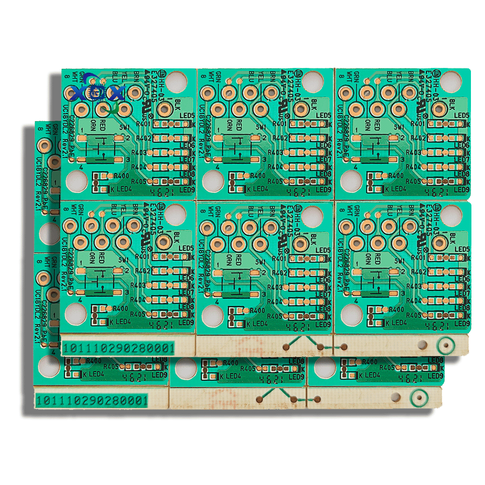
Engineered for demanding electrical environments, this 94V0 Double-Sided PCB serves as a resilient foundation for complex circuitry. It strictly complies with the UL 94V-0 vertical burn highest flame retardant rating, meaning the board will self-extinguish within 10 seconds after removal from a direct flame. This critical characteristic ensures absolute electrical and fire safety in extreme heat scenarios, providing engineers with a dependable substrate that feels rigid, structurally sound, and meticulously finished. From the smooth, uniform application of the solder mask to the precisely drilled vias, every physical detail is optimized to support stable signal transmission and long-term durability in field deployments.
The manufacturing sequence of our double-sided circuit boards relies on highly controlled chemical and mechanical processes. By maintaining strict tolerances at every fabrication stage, we ensure that the final bare board provides flawless connectivity and physical integrity for subsequent component assembly.
Through-hole metalization forms the critical conductive bridge between the top and bottom layers. The process requires exact timing and chemical balance to deposit a uniform copper layer inside microscopic drilled channels, ensuring reliable electrical pathways without structural weak points.
| Process | Key Technical Points | Precision Requirements |
|---|---|---|
| Base Material Preparation | FR-4/Aluminum substrate cutting, copper foil thickness 1-2oz (5-70μm) | Size tolerance ±0.15mm |
| Drilling | CNC mechanical drilling (hole diameter ≥0.3mm) → Dering | Hole position accuracy ±0.05mm |
| Hole Metalization | PTH (Chemical Plating): Palladium activation → Chemical electroplating (0.5-1μm) → Electroplating thickening (hole copper ≥20μm) | Deep diameter ratio ≤8:1 |
| Graphic | Double-sided LDI exposure → Graphic electroplating (copper tin protection) → Alkaline etching film removal | Line width tolerance ±0.07 |
| Solder Mask and Surface Treatment | Screen printing/spraying solder mask ink (green oil) → Character printing → HASL spray tin/ENIG gold immersion/OSP anti-oxidation | Solder mask bridge width ≥0.1mm |
For applications subjected to severe mechanical stress or heavy current loads, standard fabrication is augmented with specialized techniques. These advanced methods physically fortify the board, ensuring long-term operational stability under harsh conditions.
Selecting the appropriate base material is the most critical decision in the hardware design phase. The physical properties of the substrate dictate the board's thermal management capabilities, signal propagation speed, and structural rigidity. Below is a comprehensive comparison to guide precise material specification.
| Material Type | Dielectric Constant (Dk) | Thermal Conductivity (W/mK) | Bending Strength (MPa) | Applicable Scenarios |
|---|---|---|---|---|
| FR-4 Epoxy Board | 4.3-4.7 | 0.3 | >400 | Consumer Electronics / Industrial Control Motherboard |
| CEM-1 Composite Board | 4.5-5.0 | 0.25 | >300 | Low-cost Home Appliance Control Board |
| Aluminum Substrate | - | 1.5-4.0 | >200 | LED Lighting / Automotive Power Module |
| Polytetrafluoroethylene (PTFE) | 2.0-2.2 | 0.25 | >150 | High-frequency RF Module (<6GHz) |
The architectural transition from single-layer to double-sided routing unlocks significant performance thresholds. This configuration not only condenses the physical footprint of the hardware but also introduces robust electrical shielding and thermal pathways.
| Indicator | Double-sided Board Performance | Comparison with Single-sided Panel Improvement |
|---|---|---|
| Wiring Density | Supports cross-line, reducing jumpers | Component density increased by 50% |
| Signal Integrity | Controllable through-hole impedance (±8%), suitable for circuits below 50MHz | Interference reduction of 20% |
| Heat Dissipation Capability | Double-sided copper laying heat conduction via holes, thermal resistance reduction of 0% | Temperature rise of 15℃ (equal power consumption) |
| Reliability | Meets IPC-6012 CLASS 2 standard (industrial grade) | Lifespan >10 years (industrial environment) |
Beyond technical specifications, the double-sided architecture presents a highly rationalized financial proposition for project scaling. Our streamlined quotation and delivery workflows ensure that clients only need to submit Gerber files and BOM tables to rapidly acquire precise pricing and production schedules.
The versatility of the 94V0 Double-Sided PCB allows it to serve as the operational backbone across a vast spectrum of industries. From everyday smart devices to critical infrastructure, its balanced profile of cost, durability, and performance makes it an industry staple.
Smart Home: Highly prevalent in IoT ecosystems, providing the necessary routing density for WiFi modules (such as the ESP8266 double-sided board) and complex audio processing in Bluetooth speaker motherboards.
Portable Devices: Utilized extensively in mobile power control boards (leveraging the 2oz thick copper for safe energy transfer) and the logic controllers of e-book readers.
Beyond consumer goods, this substrate is engineered for core sectors demanding extreme thermal management and flame retardant reliability. It is widely deployed in high-power power supply modules, commercial LED lighting arrays, automotive electronic control units, and industrial automation controllers where failure is not an option.
To further reduce procurement friction and compress supply chain cycles, we provide end-to-end turnkey engineering solutions. Our factory operates under strict international compliance, holding ISO9001, IATF16949, and AS9100D certifications, thoroughly satisfying the rigorous quality mandates of the aerospace, automotive, and industrial sectors.


